Altium test point schematic symbol Top 5 benefits of using the altium schematic viewer for your Schematic capture software and pcb layout tools in altium designer| altium
Altium Schematic Flip Component
Altium researcher Altium schematic library grid Let the experts talk about : how can i see schematic and pcb in altium
Let the experts talk about : how can i see schematic and pcb in altium
Altium- schematic design common mistakesSchematic altium designer Altium schematics functionAltium document.
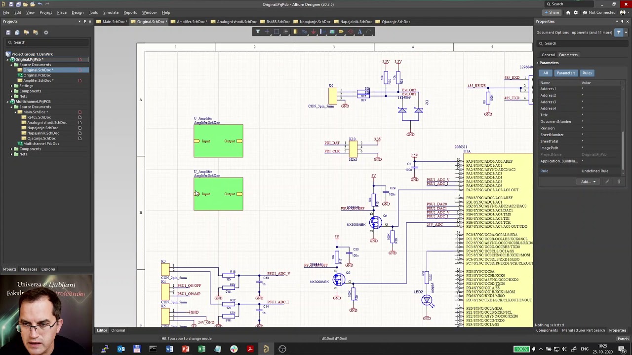
How to create a pcb schematicResolving schematic errors Altium schematics #02: copying parts of schematics with the refactorSchematic capture software and pcb layout tools in altium designer| altium.

Altium search component in schematic
Altium schematic template editAltium multi part schematic symbol Altium schematic flip componentSchematic altium designer.
Altium schematic previewAltium designer quick-start tutorial Schematic capture software and pcb layout tools in altium designer| altiumHow to create a pcb schematic.

Making connections on a schematic
Altium pcb grounds necessaryAltium schematic drc check Let the experts talk about : how do you check a drc [definitive guide]Schematic altium pcb selecting.
Altium schematic hackaday amplifierAltium pcb designer: schematic checks Altium print all schematic pagesSchematic altium component shown resolving errors properties status section bottom panel current general fig outdated needs updated.

Schematic altium highlight nets designer example pcb simplify highlighting highlighted without
1 (schematic circuit using altium designer 2017) source: researcherSchematic & netlist checks for error-free pcbs Altium search component in schematicHow to create a pcb schematic.
Altium schematic library editorHow to highlight nets to simplify schematics & pcb designs Altium designer viewerAltium schematic to pdf.


Altium- Schematic design common mistakes | by kishankrs | Medium

afrople - Blog

Schematic & Netlist Checks for Error-Free PCBs | Sierra Circuits

Making Connections on a Schematic | Altium App StartPage

Schematic Capture Software and PCB Layout Tools in Altium Designer| Altium

Altium Designer Quick-Start Tutorial | Phil's Lab | Industry Expert
Altium Search Component In Schematic

Altium Schematic Template Edit
