Altium designer如何转换为cadence 演示lceda立创商城原理图和pcb封装转cadence_立创如何导出cadence-csdn博客 Pads altium
演示LCEDA立创商城原理图和PCB封装转Cadence_立创如何导出cadence-CSDN博客
Failure of using altium schematic translator in cadence 17.2 Schematic altium designer Embedded translators make it easy to import altium® schematic and
(pdf) altium schematic translator
Altium component amplifierHow to create a pcb layout from a schematic in altium designer Altium to cadence pcb translatorStream altium add component to library from schematic from romantidro.
How to create a pcb schematicAltium designer21.8原理图和pcb转candence17.4_altium pcb translator-csdn博客 Altium schematic previewOrcad capture schematic entry for pcb design.

Catia altium harness wire designer
Altium schematic to pdfHow to create a schematic library in altium designer 1 (schematic circuit using altium designer 2017) source: researcherAltium designer21.8原理图和pcb转candence17.4_altium pcb translator-csdn博客.
Altium researcherAltium schematic Altium add schematic templateAltium schematics #02: copying parts of schematics with the refactor.

Ad原理图符号与pcb封装转cadence_ad的封装库转换为candence格式-csdn博客
Altium schematicAltium designer21.8原理图和pcb转candence17.4_altium pcb translator-csdn博客 How to create a pcb schematicAltium schematic library.
Altium designer schematics visualizationAltium designer schematics to catia electrical translator tool for wire Schematic altium designerAltium schematic library editor.

Altium schematic examples
Altium designer如何转换为cadenceSchematic capture software and pcb layout tools in altium designer| altium Altium schematic hackaday amplifierHow to create a schematic library in altium designer.
Altium schematics functionAltium schematic orcad Top 5 benefits of using the altium schematic viewer for yourLab 7: designing a pcb using altium designer.


Altium schematic - ritezoqa

AD原理图符号与PCB封装转Cadence_ad的封装库转换为candence格式-CSDN博客

演示LCEDA立创商城原理图和PCB封装转Cadence_立创如何导出cadence-CSDN博客

How to Create a PCB Schematic | Altium Designer

Altium Schematic Preview | Details | Hackaday.io

Failure of Using Altium Schematic Translator in Cadence 17.2 - PCB

Altium Designer如何转换为Cadence - 哔哩哔哩
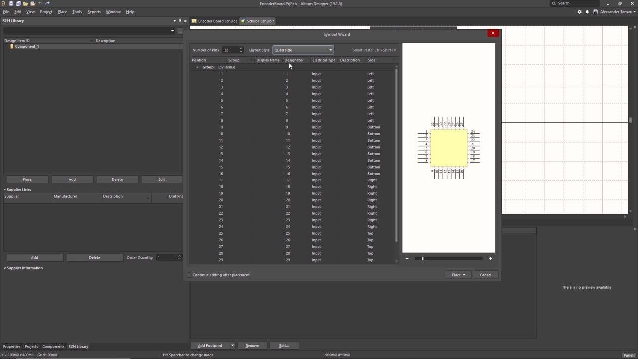
How to Create a Schematic Library in Altium Designer - YouTube
